Why does increasing temperature increase conductivity in semiconductors?
It is an empirical fact that increasing the temperature of a conductor decreases its conductivity. On Exercise 2.6.1 we provided some models for why conduction decreases as temperature increases. So, it is a puzzle that some materials show the opposite behavior! All the way back around 1833, Michael Faraday noticed this effect in $\text{AgS}$. It is also observed in pure silicon and other materials we know call semiconductors.
Before explaining why the conductivity of semiconductors increases with increasing temperature, we'll ask another equally puzzling question: why does a semiconductor like silicon conduct at all? Silicon is right below carbon on the periodic table, and it has the same diamond structure. As we saw in Exercise 13.6.1, diamond does not conduct electricity because it has full bonding orbitals and therefore no delocalized electrons. So, why does silicon, which has the same number of valence electrons and the same crystal structure as diamond, ever conduct electricity?
The answer to both of our questions will come from an expansion of the models introduced to explain why metals conduct electricity but not insulators. Before reading further take a moment to think about what might be going on. Remember that conductivity is given by the Eq. 13.8.1: $\sigma = n |e| \mu_e$. The charge of an electron isn't changing, and based on what we know from conductors, the mobility, $\mu_e$ should decrease with increasing temperature. Is it possible that increasing temperature can increase the number of free charge carriers?
Exciting Silicon Electrons
Silicon has a diamond structure. As you may recall from chemistry, the bonding orbitals of this shape are a hybrid of the $\text{s}$ and $\text{p}$ orbitals. They are called $\text{sp}^3$ orbitals. They have an energy that is in between $\text{s}$ and $\text{p}$ orbitals of which they are hybridized. Figure 13.9.1 below depicts these orbitals along with their energies.
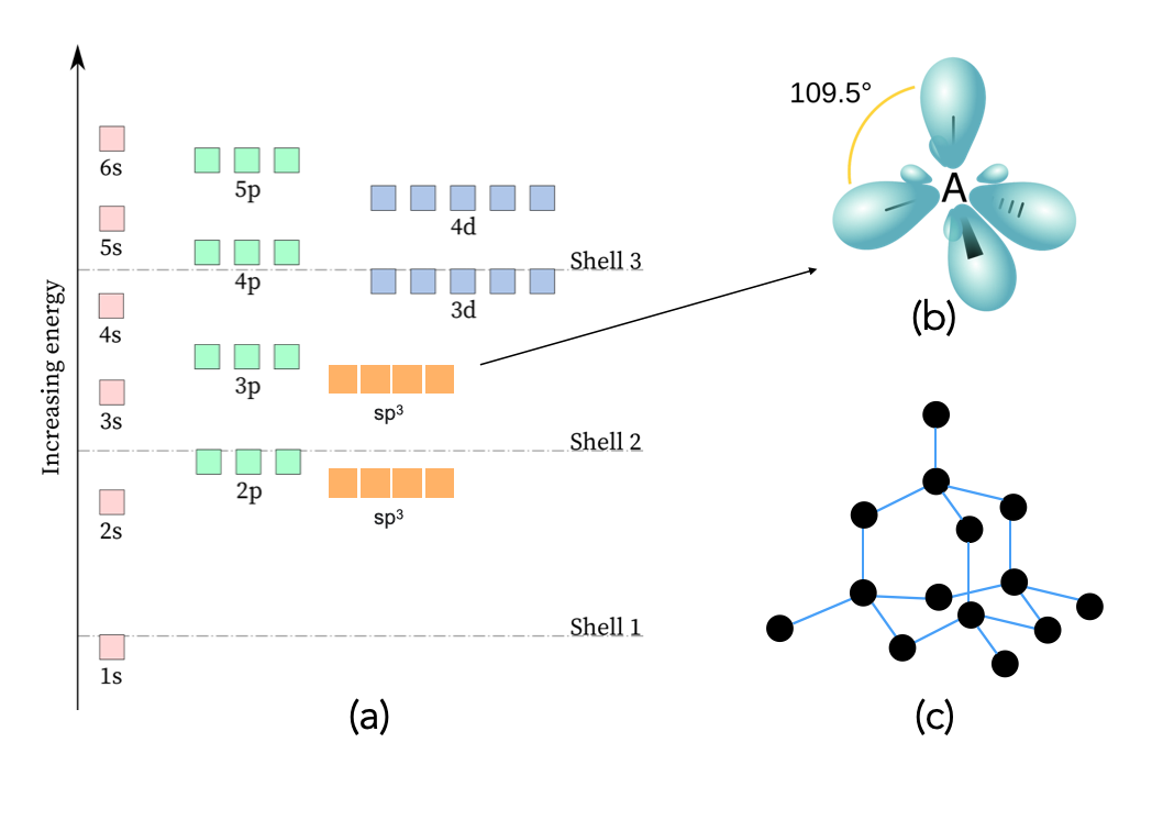
Figure 13.9.1 (a) A diagram of the energies associated with basic atomic orbitals, including the $\text{sp}^3$ hybrid orbitals between the 2s and 2p and 3s and 3p orbitals. (b) the shape of $\text{sp}^3$ orbitals. (c) A depiction of the bonding in a diamond structure of repeating atoms with $\text{sp}^3$ bonding orbitals.
In solid silicon, the ground state of the valence electrons is the $\text{sp}^3$ orbital between the $3\text{s}$ and $3\text{p}$ orbitals. What would happen if one of these electrons was excited to the next available orbital, namely $4\text{s}$? This situation is depicted in Figure 13.9.2 below. The excited electron in $4\text{s}$ orbital is depicted as a dotted circle equally spread out around the the atom. The $\text{sp}^3$ orbital it was excited from is now missing an electron and is only a fractional $\frac{1}{2}$ bond, represented as a dotted line. As soon as this happens, there is no reason for the remaining seven electrons in the $\text{sp}^3$ orbitals to stay in this unbalanced state, so they will resonate between the different structures. This can be alternatively viewed as all of the $\text{sp}^3$ bonds becoming fractional $\frac{7}{8}$ bonds.

Figure 13.9.2 (a) A depiction of the result of exciting one of the valence $\text{sp}^3$ electrons in crystalline silicon to the $4\text{s}$ orbital. The result is one $\frac{1}{8}$ fractional $4\text{s}$ bond with all the surrounding atoms and a single $\frac{1}{2}$ fractional $\text{sp}^3$ bond which can resonate with the other three $\text{sp}^3$ bonds. (b) Equivalently, all the $\text{sp}^3$ bonds can be viewed as fractional $\frac{7}{8}$ bonds. Of course, the new $4\text{s}$ bond could be viewed as a single $\frac{1}{2}$ bond which resonates between the four neighboring atoms, but this would be hard to depict without confusing the $4\text{s}$ and $\text{sp}^3$ orbitals.
We now have everything we need to answer both of our questions, and the answers are related.
First, why does silicon conduct at all, given that it has full bonding orbitals? The answer is that once an electron gets excited into a higher orbital, it is delocalized. A single electron in the $4\text{s}$ orbital of silicon behaves similarly to lithium's single electron in the $2\text{s}$ orbital depicted in Figure 13.6.4 and Figure 13.6.7. Additionally, the $\text{sp}^3$ electrons are now delocalized due to fractional bonds and they are also free to move around. However, for those electrons, it is typical to instead to think about the electron "hole" that was left behind as moving. This is depicted in Figure 13.9.3 below. The hole (the lack of an electron) has a positive charge relative to the surrounding material and moves in the opposite direction of electrons. There are few reasons to use this conceptualizations of holes for the missing electron in the valence bonding orbitals after it has been excited to higher state:
- Electrons and holes can "recombine". If an excited electron encounters a partially empty bonding orbital, it can "relax" back into it, releasing energy in the process (either thermal energy or a photon). It is a nice analogy to think about electrons "filling in" the holes, which of course gets rid of the free electron and hole.
- Typically, the valence electrons can't move. They can only move when one is missing, i.e., there is a hole. So, it is easier to talk about holes moving than valence electrons near holes.
- The electrons that move through the partially filled valence orbitals are typically not as mobile as electrons in the excited $4\text{s}$ state. With the concept of holes, we can just talk about the mobility of electrons and the mobility of holes without getting confused.

Figure 13.9.3 An animation of holes moving, i.e., of electrons moving through the partially filled valence orbitals due to resonance.
Second, why does the conductivity of semiconductors increase with increased temperature? The answer is that you need energy to excite the electrons from the valence bonding orbitals to the higher state which then allows the excited electrons and the holes to conduct electricity. This requires energy (thermal, radiation, etc.) Increasing the temperature increases the energy available for this electronic excitation.
There's an issue, though - increasing temperature should still decrease mobility (by increasing scattering. These two effects work to counter each other. This is an effect we'll discuss soon.
The band theory of solids
So far, we have explained conductivity using Pauling's model on Section 13.6, and explained semiconductivity on this page by extending his model to take into account electron excitation. In these models, we started by thinking about individual atoms and their bonds and then reasoned from there.
An alternative model based in quantum mechanics, the band model, is the basis for a lot of theoretical work in materials science and solid state physics. The details of this model are beyond the scope of this course, but some of the terminology and concepts from that model are very widespread, so it is important that you have at least heard of them. We will also use some aspects of it on later pages.
In the band model, quantum mechanics is used to calculate the allowed energies for an electron in a solid taking into account all the atoms. The result is that there are "bands" of allowed energies for the electron. These bands are analogous to the discrete energy levels of electrons in an isolated atom shown in Figure 13.9.1, but (1) they are for a whole solid instead of an isolated atom and (2) each band has many electron states in it. Figure 13.9.4 below compares a representation of the energy levels for a single atom vs for a whole solid.

Figure 13.9.4 (a) A depiction of the the allowed energies in an isolated Si atom with hybridized $\text{sp}^3$ valence orbitals (depicted by greying out the $3\text{s}$ and $3\text{p}$ orbitals). (b) A depiction of the allowed energy "bands" in solid silicon according to an energy band model. Each band is made up of many states corresponding to the number of atoms in the solid. The gap between the bonding orbitals and the next available orbital in (a) is analogous to the gap between the valence and conduction band in (b).
Figure 13.9.5 depicts hypothetical band structures for metals, semiconductors, and insulators at 0K. In the band theory of solids, a conductor conducts because the valence band is not full of electrons. This means that electrons can move between adjacent states in the valence bond. This corresponds to our explanation of electrons resonating between adjacent bonds in a metal such as Lithium with only one $2\text{s}$ electron, meaning that half of the $2\text{s}$ states are empty. Alternatively, there can be overlapping bands so that even though one band is full, it overlaps in energy with the next band, allowing electrons to travel through those adjacent energy states. This is the case, for example, in solid Magnesium which has $3\text{s}^2 3\text{s}^0$ valence electrons, but 12 nearest neighbors (HCP).
In the band model, a semiconductor only conducts when an electron is excited across the band gap, resulting in one electron in the conduction band and one hole in the valence band. This corresponds to our explanation depicted above in Figure 13.9.2. An insulator, according to the band model, simply has a very large band gap, but could conduct in theory. This is the case, in fact for diamond! Diamond can be used as a semiconductor in certain applications, but at room temperature conditions it basically never conducts electricity. Check out this paper to learn more about diamond in electronics.
Although the band model is based in quantum mechanics, it has its own limitations. For example:
- The calculations are done by "adding" an electron to a perfect and infinite lattice and calculating its allowed states. This means that interactions with defects or surfaces are not taken into account.
- Electron-electron repulsion is ignored. This leads to bad predictions in some cases.
There are various theoretical models and calculation techniques to try to deal with these limitations, but it is important to know that the band model is, like all other models, a simplification of reality.
If you are interested in learning more about various ways of explaining the difference between conductors and insulators and some of the history of these developments, the paper ‘… a metal conducts and a non-metal doesn't’ is a great overview.

Figure 13.9.5 The possible band structures for allowed electron energies at 0K for (a) metals (b) semiconductors and (c) insulators.